Silicon photonics technology enables the development of compact, multifunctional, and mass-produced integrated photonic devices. However, the design of high-performance free-form optical devices remains a challenge due to the complex light-matter interactions involved and the significant time required for electromagnetic simulation. This challenge becomes even more pronounced when designing multiple silicon photonics devices, often requiring lengthy iterative optimization. Solving the problem of inverse design for large-scale silicon photonics devices has significant research value and industrial implications for design and production.
Recently, a research group led by Associate Professor Hongyan FU from Tsinghua-Berkeley Shenzhen Institute (TBSI), Tsinghua Shenzhen International Graduate School (Tsinghua SIGS) has developed a fully automated inverse design method for large-scale multi-task silicon-based photonic devices. This method is a topological optimization method based on low-dimensional Fourier frequency domain and deep neural networks, which can quickly train deep neural networks for device design while effectively controlling the minimum feature size of the inverse-designed components, without requiring any preprepared datasets.

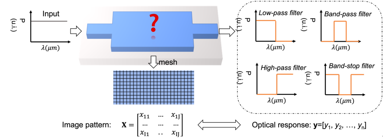
Schematic of wavelength filters on SOI platform
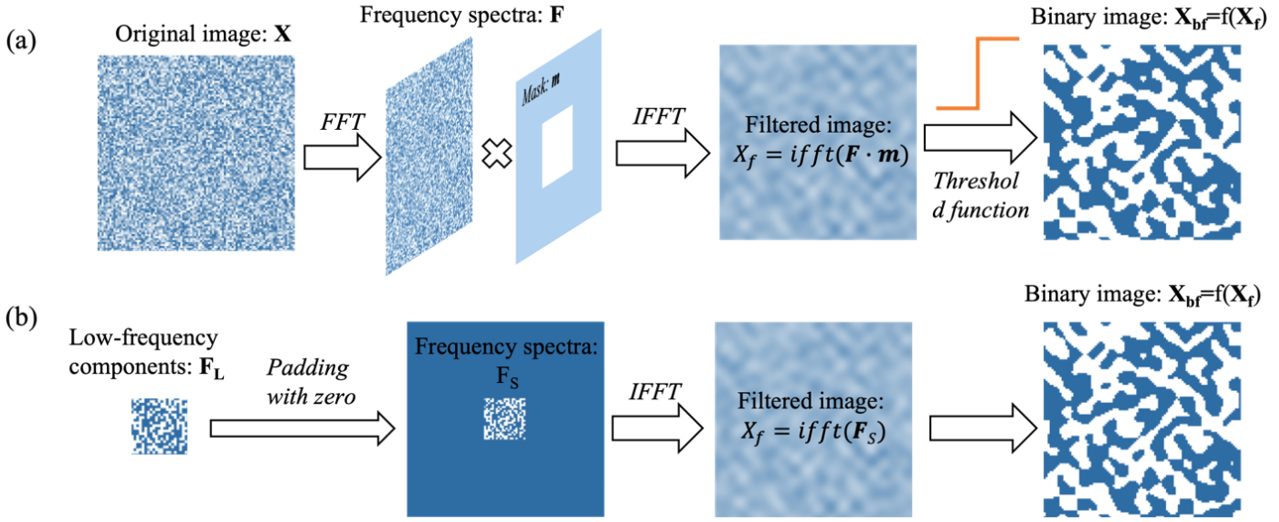
Inverse design is the process of pixelating the entire design area and determining the specific structure of the device through a goal-oriented optimization method. Considering the device processing requirements, isolated pixels and narrow gaps cannot be processed. Therefore, it is necessary to smooth the edge of the structure to meet the processing needs, which also makes some design degrees of freedom redundant. The Fourier low-frequency signal corresponds to the main structure of the device, while the Fourier high-frequency signal represents noise and rapidly changing information in the image. By using only the low-frequency Fourier component, the redundant design degrees of freedom can be reduced while controlling the minimum size of the device during the reconstruction of the time-domain image structure.

Minimal feature size control methods
To achieve multi-task device optimization design, the research team mapped the design objective to low-frequency Fourier components through a deep generative neural network. These components can be restored to the specific structure of the device graph by Fourier inverse transformation after high-frequency padding. The generated device structure is then simulated by electromagnetic simulation software to obtain the actual optical response, and the difference between the simulated response and the target optical response can be used to train the generative neural network.

Schematic of the proposed DNN-assisted topology optimization in Fourier domain for multi-task optimization
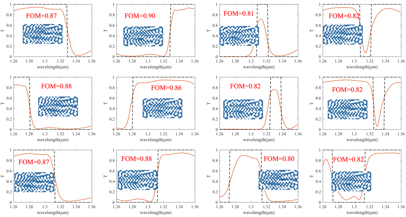
The trained neural network can be used to directly generate multiple optical devices without the need for additional optimization and simulation time. Researchers used the above-trained network for the design of optical filters. It designed 400 optical filters with high-performance metrics within less than 1 second.

Illustration of 12 randomly generated wavelength filters and their corresponding spectra.
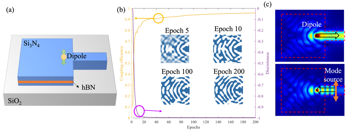
This method is almost a fully automatic multi-task optimization method, which can be easily used for the design of other free-form devices. Researchers also used this method to design an integrated single-photon source, and the efficiency of the designed integrated light source can reach over 90%. This multi-task optimization method greatly reduces the time and resources required for multi-device design, making it possible for rapid inverse design of large-scale devices in the future.

Optimization of single photon emission
The relevant research results were recently published with the title "Multi-task topology optimization of photonic devices in low-dimensional Fourier domain via deep learning" in the journal Nanophotonics. The first author of the paper is Simei MAO, a Ph.D. student from TBSI, and the corresponding author is Associate Professor Hongyan FU from TBSI. Other authors of the paper include Lirong CHENG, a Ph.D. student from TBSI, Houyu CHEN, a master's student from TBSI, Xuanyi LIU, a Ph.D. student from TBSI, and Associate Professor Qian LI from Peking University Shenzhen Graduate School. This work was supported by the Guangdong Basic and Applied Basic Research Foundation and the Science, Technology and Innovation Commission of Shenzhen Municipality.
Link to full article:
https://www.degruyter.com/document/doi/10.1515/nanoph-2022-0361/html
Writer: Simei Mao
Editors: Alena Shish, Yuan Yang, Li Han

